skip to Main Content

China Top PCB Manufacturers How to Make PCBs?

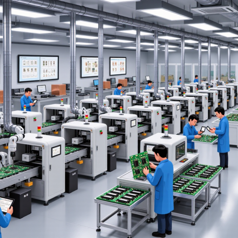
China’s top PCB manufacturers combine automated production with experienced engineering teams. This combination supports reliable boards for automotive, medical, industrial, and consumer electronics. Yet “pcb make” is not a single machine operation. It is a controlled chain of design checks, material selection, fabrication, inspection, and testing.

The process usually begins with schematics, Gerber files, stack-up planning, and design-for-manufacturing review. Engineers examine trace width, copper thickness, drill sizes, impedance, and thermal requirements. A production panel is then laminated, drilled, copper-plated, imaged, etched, solder-masked, and finished. Every stage leaves visible evidence. For example, an optical inspection system can detect a tiny missing pad before assembly begins. Electrical testing can also identify an open circuit hidden beneath the surface.

Rick Hartley, a respected PCB design educator, states, “The current will take the path of least impedance, not least resistance.” This principle explains why experienced manufacturers study return paths, plane layers, and via placement carefully. A beautiful layout can still perform poorly when its high-speed signals lack a clean reference plane.

Reliable suppliers also verify incoming laminates, monitor plating thickness, and record process results. Certifications matter, but they do not replace practical inspection. A factory may meet a standard and still miss an unclear customer requirement. That is why communication remains essential throughout pcb make projects. The strongest manufacturers ask difficult questions early, share manufacturability feedback, and provide traceable reports. Some production decisions remain imperfect, especially when cost, speed, and signal integrity conflict. This guide examines those choices and explains how leading Chinese PCB factories turn digital designs into dependable circuit boards.
China Top PCB Manufacturers How to Make PCBs?

PCB Basics and the Role of China’s Leading Manufacturers

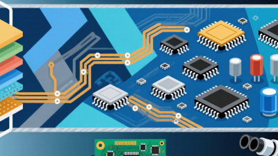
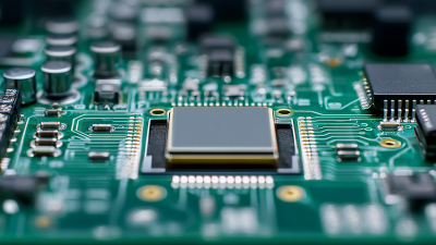
PCB basics begin with a copper-clad board, drilled holes, dielectric layers, and patterned traces. Designers control current, heat, impedance, and mechanical strength. China’s leading manufacturers add value through high-volume fabrication, multilayer pressing, laser drilling, and automated optical inspection. Prismark’s 2023 industry data estimated China produced roughly half of global PCB value. That scale supports competitive pricing and shorter production cycles. It does not remove engineering risk.

Experienced teams check stack-up drawings before tooling begins. They verify copper thickness, controlled impedance, hole tolerances, and surface finish requirements. IPC-2221 provides useful design guidance, while IPC-A-600 defines important acceptance criteria. A reliable factory also records solderability tests, microsection results, and electrical testing data. These records matter when a board enters medical, automotive, or industrial equipment. A clean schematic is not enough. I have seen small spacing errors become costly rework.

Tips: Ask for a complete DFM review before production. Confirm material certificates and test methods in writing. Request sample cross-sections for complex multilayer boards. Leave extra copper around heat-producing components. Do not assume the lowest quotation reflects the lowest total cost. Some specifications remain unclear, even after several revisions.

PCB Design, Circuit Layout, and Production Preparation

China Top PCB Manufacturers: How to Make PCBs?

PCB production begins with a clear schematic and a practical design target. A reliable workflow connects circuit layout with manufacturing requirements. Engineers define board size, layer count, materials, operating voltage, and expected current. They also check component availability and thermal limits before routing. A clean schematic is not enough.

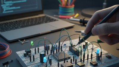
During circuit layout, place critical components close together. Keep high-speed traces short and controlled. Use consistent widths for power paths. Add ground planes where signal integrity requires them. Place decoupling capacitors beside power pins, not several centimeters away. Separate noisy switching areas from sensitive sensor circuits. Small errors matter. I have seen a poorly placed connector force an expensive redesign.

Production preparation turns design data into usable factory instructions. The package should include verified fabrication files, drill data, a bill of materials, assembly drawings, and test-point locations. Confirm the layer stack-up, copper thickness, solder mask clearance, and impedance targets. Manufacturers review these details through design-for-manufacturing checks. They may question narrow spacing, unsupported holes, or parts with uncertain supply. That feedback often improves reliability, although it can expose rushed decisions.

Before release, compare the final files with the approved schematic. Check reference designators, polarity marks, and mounting holes manually. Automated checks help, but they cannot replace engineering judgment. I still revisit every critical net because one overlooked change can survive several software checks. A small prototype run can reveal assembly distortion, heat buildup, or connector interference before full production.

Materials and Technologies Used in PCB Manufacturing

China Top PCB Manufacturers: How to Make PCBs?

Experienced PCB manufacturers begin with material selection, not machines. Most rigid boards use copper-clad FR-4 laminate for strength and stable electrical performance. Flexible circuits often use polyimide because it bends without cracking easily. Aluminum substrates can move heat away from power components. Copper foil forms the conductive paths, while resin binds the board layers during lamination. Material thickness affects impedance, heat flow, and mechanical strength.

Manufacturing starts with computer-controlled imaging, which transfers circuit patterns onto copper surfaces. Chemical etching removes unwanted copper, leaving the designed traces. Plated-through holes connect different layers. Microvias support compact high-density designs, but they require strict drilling and plating control. Solder mask protects exposed copper from oxidation and accidental bridging. Silkscreen adds reference marks for assembly and inspection.

Quality teams use automated optical inspection, electrical testing, and cross-section analysis. They also measure trace width, hole size, layer alignment, and impedance. In practical production, small variations still appear. A board may pass basic testing yet show weakness near a hot connector. That finding should change material choices or copper weight. Cleaner processes help, but no production line is flawless. Engineers must review real test data, not rely only on design software. Good manufacturers document each batch, control moisture, and trace process changes carefully.

China Top PCB Manufacturers: How to Make PCBs?

Copper foil thickness is specified by copper weight. The values below show commonly used nominal copper thicknesses in PCB manufacturing, calculated from approximately 35 µm per ounce of copper.

Thicker copper improves current-carrying capacity and heat dissipation, while lighter copper supports finer traces and higher-density PCB designs. Actual finished thickness can vary because of plating and manufacturing tolerances.

Step-by-Step PCB Fabrication and Assembly Process

China Top PCB Manufacturers: How to Make PCBs?

Step-by-Step PCB Fabrication and Assembly Process

PCB production starts with a verified design package. Engineers review Gerber files, drill data, stack-up drawings, and component lists. Design-for-manufacturing checks catch narrow traces, weak clearances, and difficult component spacing. A second review is worthwhile. Small omissions can create expensive delays.

The factory cuts copper-clad laminate to panel size. It cleans the surface before applying dry film and imaging the circuit pattern. Chemical etching removes unwanted copper, while inspection systems check trace widths and open circuits. Layered boards are aligned, laminated under heat, and drilled with controlled tools. Plated holes then receive copper to connect the layers. The process is precise, but alignment can still drift. Experienced technicians verify registration at this stage.

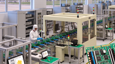
Solder mask protects exposed copper, leaving pads ready for assembly. Silkscreen markings identify reference points and polarity. Electrical testing checks continuity and isolation before components arrive. During SMT assembly, a stencil applies solder paste, a placement machine positions parts, and a reflow oven bonds them to the board. Through-hole parts may require selective soldering. AOI and sample testing follow. Manufacturing records, operator checks, and retained samples improve traceability. One practical lesson remains clear: speed should never replace inspection.

China Top PCB Manufacturers How to Make PCBs? - Step-by-Step PCB Fabrication and Assembly Process
Step Manufacturing Stage 主要目的 / Main Purpose Typical Materials or Equipment Typical Process Data Quality Control Focus
1 Design Review and DFM Check Verify that the PCB layout can be manufactured and assembled reliably before production begins. Gerber files, drill files, pick-and-place data, bill of materials, design-rule software. Typical checks include trace width, spacing, annular ring, drill-to-copper clearance, solder-mask clearance, and component orientation. Data completeness, manufacturability, electrical rules, component availability, and consistency between fabrication and assembly files.
2 Material Selection and Cutting Prepare the laminate panels used to build the circuit board. FR-4 laminate, copper-clad panels, CNC routing or panel shearing equipment. Common FR-4 constructions use glass-reinforced epoxy laminate with copper foil commonly ranging from 18 to 70 micrometres for standard boards. Laminate thickness, copper thickness, surface condition, moisture protection, and panel dimensions.
3 Inner-Layer Imaging Transfer the inner-layer circuit pattern onto copper-coated laminate. Dry film photoresist, imaging system, ultraviolet exposure unit, cleanroom processing area. The photoresist is exposed according to the circuit image, then developed to reveal the copper areas that will be etched or retained. Line definition, registration accuracy, photoresist adhesion, and absence of dust or pinholes.
4 Etching and Inner-Layer Inspection Remove unwanted copper and inspect the completed inner-layer circuitry. Alkaline or acidic etching line, stripping equipment, automated optical inspection system. Etching removes exposed copper while the remaining copper forms the intended traces, pads, and planes. Short circuits, open circuits, over-etching, under-etching, conductor width, and inner-layer registration.
5 Lamination Build the multilayer PCB by bonding inner layers, prepreg, and copper foil under heat and pressure. Prepreg, copper foil, stainless-steel plates, lamination press, controlled-temperature heating system. Heat and pressure cure the resin in the prepreg and create a solid multilayer structure. The exact cycle depends on resin system and board construction. Layer alignment, resin fill, dielectric thickness, voids, delamination, and overall board thickness.
6 Drilling and Hole Preparation Create through-holes, blind vias, buried vias, and component holes required by the design. CNC drilling machines, laser drilling equipment for selected microvias, drill bits, desmear line. Hole diameter and position are controlled according to the drill file. Desmear removes resin residue from hole walls after drilling. Hole location, hole size, wall condition, burrs, resin smear, and drill-to-copper clearance.
7 Copper Plating and Outer-Layer Patterning Make the drilled holes electrically conductive and form the outer-layer circuit pattern. Electroless copper process, electrolytic copper plating line, dry film, exposure and etching equipment. A thin electroless copper layer provides initial conductivity, followed by electrolytic copper plating to build the required barrel and surface copper thickness. Plating coverage, hole-wall continuity, copper thickness, trace definition, adhesion, and electrical continuity.
8 Solder Mask and Surface Finish Protect exposed copper and prepare solderable pads for component assembly. Liquid photoimageable solder mask, ultraviolet exposure system, hot-air or chemical surface-finish equipment. Common finishes include HASL, lead-free HASL, electroless nickel immersion gold, immersion silver, and immersion tin. The selected finish depends on application and soldering requirements. Pad coverage, solder-mask registration, surface flatness, oxidation resistance, coating uniformity, and solderability.
9 Legend Printing, Routing, and Electrical Testing Add identification markings, separate the boards from the production panel, and verify circuit connectivity. Inkjet or screen printer, CNC router, V-cut machine, flying-probe tester or fixture-based tester. Testing checks for opens and shorts. Depanelization may use routing or V-scoring depending on board shape and assembly requirements. Netlist conformity, board outline, dimensional accuracy, marking readability, edge quality, and electrical test results.
10 Solder Paste Printing Apply a controlled amount of solder paste to the PCB pads before component placement. Stainless-steel stencil, solder paste, automatic screen printer, solder-paste inspection system. Stencil thickness and aperture design are selected according to pad geometry and component pitch. Paste volume and alignment are monitored after printing. Paste height, area, volume, alignment, bridging risk, insufficient deposits, and stencil cleanliness.
11 SMT Component Placement Place surface-mount components accurately onto the printed solder paste. Pick-and-place machine, feeders, vacuum nozzles, component reels, trays, and moisture-sensitive-device controls. Placement accuracy depends on package type, machine capability, fiducial quality, and feeder condition. Components are placed according to centroid and rotation data. Component identity, polarity, orientation, placement position, missing parts, wrong parts, and feeder setup.
12 Reflow Soldering Heat the assembled PCB so the solder paste melts and forms permanent solder joints. Multi-zone reflow oven, thermocouples, nitrogen system when required, profile-analysis software. The temperature profile is matched to the solder-paste specification and component limits. Peak temperature and time above liquidus vary by solder alloy and assembly design. Solder joint wetting, voiding, tombstoning, bridging, component damage, board warpage, and thermal-profile compliance.
13 Through-Hole Assembly and Wave or Selective Soldering Install and solder components with leads that pass through the PCB. Manual insertion tools, insertion fixtures, wave-soldering machine, selective-soldering system, soldering irons. Selective soldering is used when only specific through-hole locations require solder, while wave soldering can process suitable groups of through-hole joints. Lead protrusion, solder fill, solder bridges, insufficient solder, component seating, polarity, and thermal damage.
14 Inspection, Cleaning, and Functional Testing Confirm assembly quality and verify that the product performs its intended electrical functions. AOI, X-ray inspection, microscope, in-circuit tester, functional test fixture, cleaning equipment. Inspection methods may include visual inspection, AOI, X-ray for hidden joints, in-circuit testing, and powered functional testing. Solder-joint quality, component presence, polarity, hidden-joint integrity, electrical performance, and workmanship requirements.
15 Final Quality Review and Packaging Release conforming PCBs or assemblies for shipment while protecting them from moisture, static electricity, and mechanical damage. ESD-safe packaging, moisture-barrier bags, desiccant, humidity indicator cards, labels, and final inspection records. Packaging requirements depend on component moisture sensitivity, board surface finish, storage conditions, and transportation distance. Traceability, quantity, cosmetic condition, test records, packaging integrity, ESD protection, and shipment documentation.
Note: Actual process settings, tolerances, materials, and inspection criteria vary according to PCB layer count, stack-up, copper weight, component package, surface finish, solder alloy, and applicable customer or industry requirements.

Quality Testing and Choosing a Reliable Chinese PCB Manufacturer

Making a PCB requires more than routing tracks and ordering boards. A reliable Chinese PCB manufacturer should control each production stage, from material inspection to final packaging. Engineers usually review stack-up data, copper thickness, drill sizes, and impedance requirements before fabrication begins. Automated optical inspection can detect missing pads and unwanted bridges. Flying-probe testing checks electrical continuity and isolation. For complex boards, microsection analysis verifies plated-hole quality.

Testing should match the product’s risks. High-speed designs may require impedance testing with a time-domain reflectometer. Power boards need thermal and load checks. Cleanliness testing can reveal ionic residue around fine-pitch components. Ask for test records, calibration dates, and acceptance criteria. Small defects matter.

Choosing a dependable supplier requires evidence, not attractive promises. Review process certifications, equipment lists, operator training, and traceability procedures. Request a pilot batch before approving larger production. Compare the delivered boards with the approved Gerber files and drawings. A factory should explain nonconforming results clearly and provide corrective-action reports. It should also support design-for-manufacturing reviews before tooling starts.

Communication quality is easy to underestimate. Confirm tolerances, packaging, lead times, and change-control rules in writing. A capable supplier will question an unclear via design instead of silently making assumptions. Still, no factory is perfect. Test coverage may miss an unusual field failure, and samples cannot represent every production condition. Independent inspection can add confidence when the board is safety-critical. Reliable decisions come from repeated evidence, open records, and practical verification.