Top PCB Prototyping Techniques to Watch in 2025 for Innovative Designs
As the landscape of electronics continues to evolve rapidly, accessible and innovative PCB prototyping techniques are becoming essential for designers seeking to stay ahead. With the demand for faster product development and the necessity for high-quality prototypes, the advancements in PCB prototyping are capturing the attention of engineers and hobbyists alike. By 2025, several groundbreaking methods are expected to redefine how prototypes are created, dramatically impacting the design workflow and efficiency.
In this era of technological advancement, PCB prototyping not only facilitates the testing of new concepts but also allows for the integration of features that cater to the ever-growing complexities of modern electronics. Embracing these emerging techniques can foster creativity and lead to the development of innovative designs that meet the specific needs of users. As we explore the most promising PCB prototyping techniques slated for the near future, it is crucial to understand their potential contributions to the electronic design process and how they align with the trends shaping the industry.
Emerging PCB Prototyping Techniques Transforming Innovative Design
The landscape of PCB prototyping is evolving rapidly, driven by advancements in technology and the ever-growing demand for innovative designs. Among the emerging techniques,
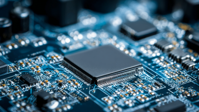
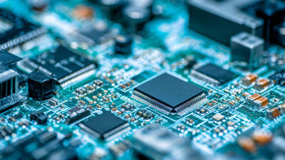
3D printing stands out as a revolutionary method that allows for the rapid production of complex PCB geometries. This technique not only shortens the development cycle but also enhances design flexibility,
enabling engineers to experiment with unconventional shapes and features that were previously challenging to achieve. Furthermore, the integration of
conductive inks in 3D printing processes opens up new possibilities for creating lightweight and compact electronic circuits, catering to the needs of modern electronic devices.
Another noteworthy trend in PCB prototyping is the adoption of machine learning algorithms for design optimization. These algorithms analyze vast amounts of data to predict potential failures and suggest improvements,
thus minimizing design iterations and time spent on testing. This proactive approach allows designers to create more reliable and efficient PCBs while reducing material waste.
As these techniques mature, they are set to redefine the boundaries of what's possible in PCB design, fostering innovation across various industries, from consumer electronics to automotive applications.
With the convergence of these advanced methodologies, the future of PCB prototyping promises to be both exciting and transformative.
Impact of Advanced Materials on PCB Prototyping in 2025
As we look towards 2025, the impact of advanced materials on PCB prototyping is poised to revolutionize the way designers approach circuit board development. With the emergence of innovative substrates, such as flexible and high-frequency laminates, prototyping will not only become more efficient but also enable the creation of more complex and compact designs. These advanced materials can withstand higher thermal and electrical stresses, allowing for reliable performance in critical applications, thus pushing the boundaries of what is possible in electronic design.
Moreover, the integration of smart materials and composites into PCB prototyping will be a game changer. These materials can adapt to environmental changes and enhance functionality, paving the way for self-sensing and self-healing circuits. Such advancements will not only streamline the prototyping process but also lead to the development of eco-friendly solutions, reducing waste and improving sustainability within the electronics industry. As designers embrace these cutting-edge materials, we can expect significant advancements in both performance and innovation, marking a new era in PCB prototyping.
Integration of AI and Automation in PCB Design and Prototyping
The integration of AI and automation in PCB design and prototyping is set to revolutionize the industry by 2025. As companies strive for efficiency and innovation, these technologies are enabling designers to streamline workflows and reduce the time it takes to bring new products to market. AI-driven design tools can analyze vast amounts of data to identify optimal circuit layouts and component placements, while automated processes help in quickly fabricating prototypes with precise specifications.
Tip: To get started with AI integration in your PCB design, consider utilizing machine learning algorithms that can predict potential design flaws early in the process. This predictive capability not only saves time but also enhances the overall quality of the designs.
Moreover, automation supports rapid prototyping techniques that can adapt to changes in design in real-time. This flexibility allows engineers to experiment with innovative concepts without the risk of extensive rework. Automated testing and validation processes further ensure that the prototypes meet the required standards before moving to mass production.
Tip: Implementing a modular design approach can greatly enhance the benefits of automation. By breaking down complex systems into smaller, manageable modules, you can easily adapt designs and utilize automation for efficient assembly and testing.
Top PCB Prototyping Techniques to Watch in 2025 for Innovative Designs
| Technique |
Description |
Benefits |
Expected Impact |
| AI-Driven Design Automation |
Utilization of AI algorithms to automate complex design processes and enhance decision-making. |
Reduces time to market; improves design accuracy; lowers costs. |
High efficiency gains; trend towards smart manufacturing. |
| 3D Printing for Prototyping |
Using additive manufacturing to create PCB prototypes rapidly. |
Faster iterations; reduced material waste; design flexibility. |
Increased speed in prototype development; enabling complex geometries. |
| IoT Integration in PCB Design |
Embedding IoT features directly into PCB designs for seamless connectivity. |
Enhanced functionality; better performance tracking; real-time data collection. |
Increasing demand for connected devices; driving innovation. |
| Advanced Simulation Software |
Tools that simulate electrical performance and thermal effects of PCB designs. |
Early detection of issues; optimization of designs before production. |
Improved reliability of products; cost savings through reduced revisions. |
| Automated Testing and Inspection |
Use of robotics and AI for quality assurance in PCB manufacturing. |
Higher consistency; reduced human error; faster testing times. |
Enhanced product quality; increased consumer trust. |
Sustainability Trends in PCB Manufacturing and Prototyping Techniques
Sustainability has become a critical focus in PCB manufacturing, with companies increasingly adopting eco-friendly practices to reduce their environmental impact.
In 2025, we can expect to see a shift toward utilizing recyclable materials and energy-efficient processes.
This trend not only enhances the sustainability of PCB production but also appeals to environmentally conscious consumers and industries.
As the demand for greener solutions rises, designers will need to integrate these sustainable materials into their prototyping techniques, enhancing both functionality and eco-friendliness.
To thrive in this evolving landscape, consider implementing the following tips:
First, prioritize the use of biodegradable substrates and low-impact manufacturing processes in your prototyping efforts.
This can significantly reduce waste and resource consumption.
Second, leverage digital technologies for rapid prototyping.
Advanced software tools can help you optimize designs for sustainability while minimizing material usage.
By adopting these innovative practices, you can ensure that your PCB designs are not only cutting-edge but also align with the growing trend towards sustainability.
As we look ahead to 2025, collaboration with suppliers committed to sustainable practices is essential.
Building partnerships with those who share your values can lead to more significant advancements in eco-friendly PCB solutions.
Engaging in sustainable supply chain practices will not only improve the ecological footprint of your projects but also foster a community of innovation that prioritizes the health of our planet in PCB design.
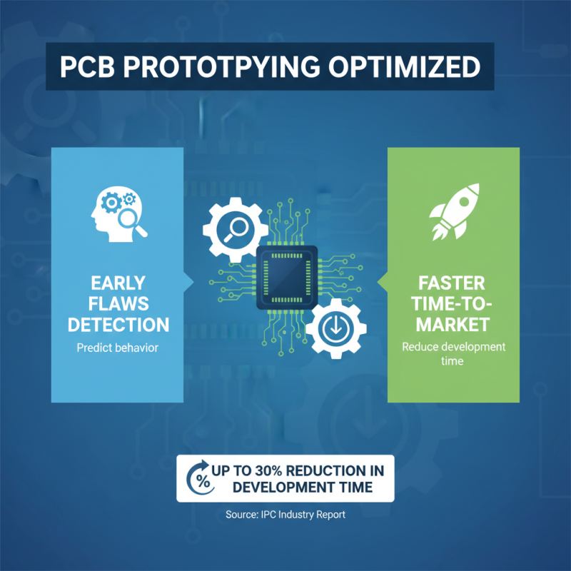
The Role of Simulation Tools in Enhancing PCB Prototyping Efficiency
In recent years, simulation tools have become indispensable in enhancing PCB prototyping efficiency. As designs grow more complex, the use of advanced simulation software allows engineers to predict the behavior of prototypes under various conditions, thereby identifying potential flaws early in the design process. According to a recent industry report by IPC, companies that integrate simulation tools into their prototyping processes can reduce development time by up to 30%, leading to faster time-to-market and significant cost savings.
One of the key advantages of simulation in PCB design is its ability to facilitate iterative testing without the need for physical prototypes, which can be resource-intensive. In fact, a study by Gartner found that organizations utilizing simulation tools effectively can cut prototype iterations by as much as 50%. This capability not only accelerates the development cycle but also enhances overall product quality, ensuring that designs meet stringent performance standards before they reach the manufacturing stage.
**Tip:** To maximize the benefits of simulation tools, engineers should invest time in training and familiarize themselves with the latest features and functionalities. This approach not only enhances productivity but also opens opportunities for more innovative design solutions. Additionally, seeking collaborative tools that allow real-time feedback from multiple stakeholders can further streamline the prototyping process.