Mastering PCB Prototyping Techniques for Beginners in Electronics
In today's rapidly evolving electronics landscape, PCB prototyping has become a crucial step in the product development cycle. According to a recent industry report by IPC, the global PCB market is expected to reach $85 billion by 2027, driven largely by advancements in technology and the demand for miniaturized devices. The prototyping phase allows engineers and designers to test their concepts and iterate designs efficiently before full-scale production. As beginners enter this field, mastering effective PCB prototyping techniques is essential for reducing time-to-market and minimizing costs. By understanding the fundamentals of PCB design, fabrication, and testing, newcomers can significantly enhance their productivity and innovation capabilities in electronics. This blog aims to provide valuable solutions and insights into the best practices for PCB prototyping, setting a solid foundation for aspiring electronics enthusiasts.

Common Issues in PCB Prototyping: Understanding the Basics
 Prototyping printed circuit boards (PCBs) is a crucial step in the electronic design process, yet beginners often face a myriad of challenges. Common issues such as misalignment, improper soldering, and design errors can lead to costly delays and project setbacks. According to a report by IPC, nearly 30% of PCB rework is due to design flaws, highlighting the importance of mastering the basics before diving into prototyping.
To avoid these pitfalls, it is essential for beginners to familiarize themselves with essential prototyping techniques. For instance, utilizing a robust design software can minimize errors; tools like Altium Designer or KiCAD offer features like automatic design rule checks to ensure your layout meets manufacturing standards. Additionally, practicing proper soldering techniques can significantly reduce the likelihood of connection failures—a leading cause of prototype malfunctions.
Tip: Always double-check your PCB design against the schematic to ensure that all components are placed correctly. Another invaluable piece of advice is to prototype with lower-cost materials initially to test designs without incurring high expenses before moving on to production-grade PCBs. This approach allows you to iterate quickly and gather vital feedback for future designs.
Identifying Design Flaws: Key Challenges for Beginners
Identifying design flaws in PCB prototyping can be one of the most daunting challenges for beginners in electronics. As novice designers embark on creating their first printed circuit boards, they often overlook critical aspects such as component placement, trace routing, and signal integrity. Each of these elements plays a significant role in the functionality and performance of the final product. For instance, improper spacing between traces can lead to short circuits or electromagnetic interference, which can ultimately derail an otherwise well-thought-out design.
Another common pitfall is not accounting for the physical layout of components. Beginners may fail to consider how components will interact with one another thermally and physically, leading to overheating or mechanical clashes. It's essential to simulate how the PCB will behave in real-world conditions, taking into account factors like heat dissipation and the mechanical resilience of the board. By focusing on these challenges and learning to identify potential flaws early in the design process, beginners can significantly improve their PCB prototypes, paving the way for successful electronics projects.
Troubleshooting Soldering Problems in PCB Prototypes
Soldering is a critical skill in PCB prototyping, and troubleshooting common soldering problems can significantly enhance your project outcomes.
One frequent issue is cold solder joints, which occur when solder does not melt properly or is not heated adequately. This can lead to weak connections that may fail under heat or vibration. To combat this, ensure your soldering iron is adequately heated before applying it to the joint. Always use the right type of solder; for electronics, a lead-free solder tends to provide better results.
Another challenge in soldering is bridging, where solder unintentionally connects two adjacent pads, leading to short circuits. Achieving precision with your soldering technique is key here. Use a finer soldering tip to maintain control and apply solder judiciously. If a bridge does form, desoldering pumps or wick can be employed to remove excess solder efficiently. With practice and attention to detail, you can refine your soldering skills, making your PCB prototypes more reliable and effective.
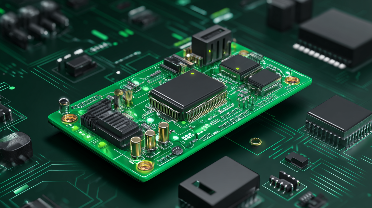
Managing Component Placement for Optimal Performance
Effective component placement is crucial in PCB design, as it can significantly influence the performance and reliability of electronic devices. According to a report by IPC, approximately 70% of PCB-related failures can be traced back to issues in placement, soldering, and routing. Therefore, mastering component placement techniques is essential for beginners looking to create efficient and functional prototypes.
 When managing component placement, consideration of the signal flow is paramount. High-speed components should be placed closer together to minimize the length of traces, which can help reduce electromagnetic interference and improve signal integrity. Additionally, following the best practices outlined by the Institute of Electrical and Electronics Engineers (IEEE) can help in achieving optimal arrangements. Their guidelines suggest keeping power and ground planes close to the components to minimize the inductance and improve overall performance.
 Another critical aspect of component placement involves thermal management. According to a study by the Electronics Industry Association, improper thermal management can lead to a performance degradation of up to 50% in high-power circuits. Ensuring adequate spacing between heat-generating components and utilizing thermal vias can greatly enhance heat dissipation, thereby prolonging the lifespan of the PCB and its components. Attention to these details during the prototyping phase ultimately lays a solid foundation for successful product development.
Electrical Testing Techniques to Validate PCB Functionality
Electrical testing is a critical step in validating the functionality of printed circuit boards (PCBs), especially for beginners entering the electronics field. According to a report by SEMI, approximately 80% of PCB-related failures can be traced back to design and testing issues. This underscores the importance of adopting effective electrical testing techniques to ensure that the prototypes not only function as intended but also meet the quality standards required for reliable performance.
One widely used testing method is the In-Circuit Testing (ICT), which can identify faulty components by measuring the electrical signals directly on the PCB. A survey by IPC indicated that the implementation of ICT can reduce production errors by up to 50%, significantly enhancing the overall efficiency of the manufacturing process. Additionally, functional testing, which assesses the operation of the assembled PCB under normal working conditions, should also be a priority. By encompassing these testing techniques, beginners can master the essential skills needed to develop successful prototypes, ultimately leading to more robust and reliable electronic products.
Mastering PCB Prototyping Techniques for Beginners in Electronics - Electrical Testing Techniques to Validate PCB Functionality
| Technique |
Description |
Tools Required |
Effectiveness |
| Functional Testing |
Testing the PCB to ensure all components are working as intended. |
Multimeter, Oscilloscope |
High |
| Visual Inspection |
Inspecting the board for visible defects such as soldering issues. |
Magnifying Glass, LED Lamp |
Moderate |
| In-Circuit Testing (ICT) |
Testing individual components on the PCB while assembled. |
ICT Fixture, Tester |
High |
| Boundary Scan |
Using boundary scan techniques to test connectivity without physical access. |
Boundary Scan Tools |
High |
| Thermal Imaging |
Detecting overheating components through thermal imaging technology. |
Thermal Camera |
Moderate |