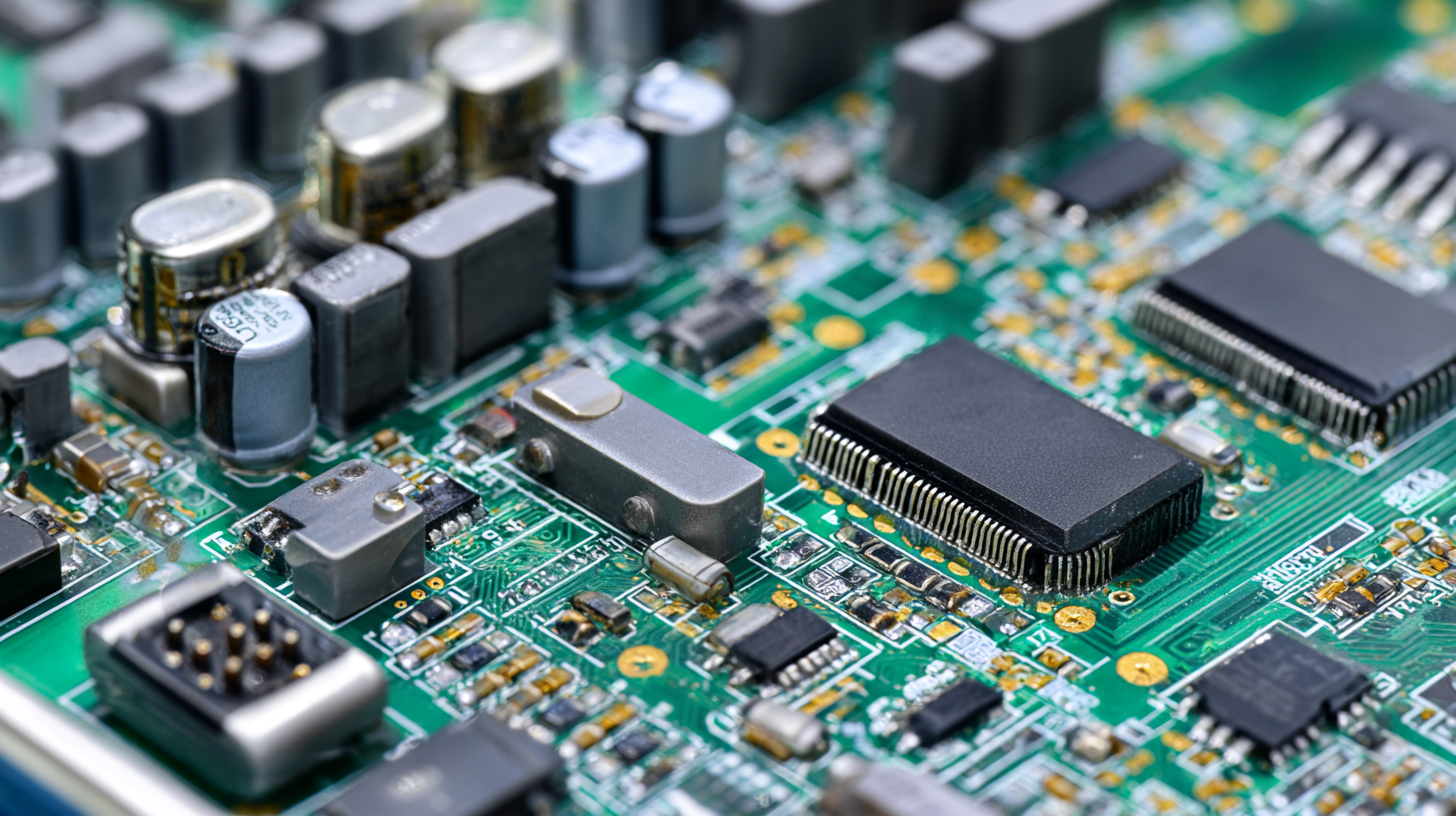
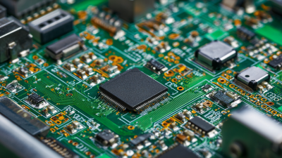
Top 5 Insights for Successful PCB Production in Modern Electronics
In the rapidly evolving landscape of modern electronics, achieving successful PCB production is essential for any manufacturer aiming to stay competitive. With the increasing complexity of electronic devices and the demand for higher performance, understanding the intricacies of the PCB production process has never been more crucial. Innovations in materials, design methodologies, and production technologies are reshaping the industry, prompting engineers and manufacturers to adapt their strategies to meet new challenges.
This article delves into the top five insights that are pivotal for successful PCB production in today's market. From leveraging advanced design software to implementing efficient manufacturing techniques, the focus will be on how these practices can lead to reduced costs, improved quality, and expedited time-to-market. By harnessing these insights, manufacturers can not only meet the growing demands of the electronics sector but also pave the way for future innovations in PCB technology.
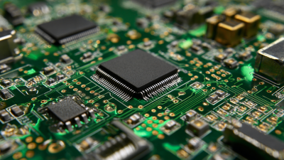
Understanding Advanced Design Techniques for PCB Layout Optimization
In the realm of modern electronics, the importance of optimized PCB layout cannot be overstated. Advanced design techniques play a crucial role in enhancing performance, reducing costs, and speeding up production times. One essential approach is the use of simulation tools that allow designers to visualize electromagnetic interference and thermal effects before physical production begins. This proactive step helps in mitigating potential issues that could arise during the production phase.
**Tip:** Always prioritize signal integrity by minimizing trace lengths and maintaining appropriate spacing between signal and ground layers. This ensures that high-frequency signals can travel without degradation, which is vital for maintaining overall circuit performance.
Another valuable technique is the implementation of modular design principles. Designing PCBs in smaller, manageable sections not only simplifies the layout process but also facilitates easier troubleshooting and upgrades in the future. By using a modular approach, engineers can quickly isolate issues and replace specific sections without the need for a complete redesign.
**Tip:** Incorporate adequate test points in your design to allow for convenient access during testing phases, making it easier to validate performance and functionality after production. This attention to detail can significantly reduce downtime and enhance overall efficiency in the PCB production workflow.
Top 5 Insights for Successful PCB Production
Incorporating Sustainable Practices in PCB Manufacturing Processes
In today’s rapidly evolving electronics industry, the push for sustainability in Printed Circuit Board (PCB) manufacturing processes has become imperative. By adopting eco-friendly practices, manufacturers not only reduce their environmental impact but also enhance their competitive edge. This shift involves the use of non-toxic materials and chemicals throughout the production cycle, minimizing hazardous waste and facilitating recycling at the end of a product's lifecycle. Innovations such as lead-free soldering and biocompatible substrates exemplify this trend toward greener manufacturing.
Moreover, implementing energy-efficient technologies can significantly decrease the carbon footprint associated with PCB production. Techniques such as utilizing renewable energy sources and optimizing supply chains contribute to lowering emissions. Incorporating automated systems also aids in reducing material waste and enhancing overall process efficiency. As consumer demand shifts towards environmentally responsible products, PCB manufacturers that embrace these sustainable practices not only align with market expectations but also pave the way for long-term viability in the electronics sector.
Leveraging Automation and AI for Enhanced Production Efficiency
In the rapidly evolving landscape of modern electronics, leveraging automation and artificial intelligence (AI) is essential for enhancing production efficiency in printed circuit board (PCB) manufacturing. AI-driven technologies enable manufacturers to tackle complex challenges by optimizing processes through predictive maintenance and automated quality control. By harnessing vast amounts of data, companies can make informed decisions that lead to a more responsive and agile production environment.
Automation not only streamlines repetitive tasks but also integrates advanced robotics and algorithmic systems that significantly reduce production time and costs. For instance, intelligent systems enable real-time monitoring of production lines, ensuring consistent quality and swift identification of potential issues. As the industry embraces these innovations, manufacturers can expect improved operational efficiency and the ability to meet the increasing demands of the market without compromising quality or reliability.
Top 5 Insights for Successful PCB Production in Modern Electronics - Leveraging Automation and AI for Enhanced Production Efficiency
| Insight |
Description |
Benefits |
Implementation Example |
| Automated Design Verification |
Utilizing AI-driven tools to check design rules and constraints automatically. |
Reduces design errors and speeds up the design process. |
Integration of EDA tools with AI capabilities. |
| Predictive Maintenance |
Using IoT sensors and AI analytics to predict equipment failures before they occur. |
Minimizes downtime and repair costs. |
Real-time monitoring systems implemented on production lines. |
| Data-Driven Decision Making |
Analyzing production data to optimize processes and reduce waste. |
Improved operational efficiency and cost savings. |
Implementing data analytics platforms integrated with production software. |
| Flexible Manufacturing Systems |
Adapting production lines to handle varying product types and volumes. |
Increases scalability and responsiveness to market demands. |
Deployment of automated assembly lines with modular equipment. |
| Enhanced Quality Control |
Implementing machine vision systems for real-time inspection of PCB assemblies. |
Reduces defects and improves product quality. |
Integration of inline inspection systems with AI for defect recognition. |
Navigating Material Selection for High-Performance PCBs
The trend toward miniaturization in electronics is fundamentally transforming the landscape of PCB production, enhancing both efficiency and reliability. As the demand for smaller, more powerful, and feature-rich devices intensifies, the design of printed circuit boards (PCBs) must evolve to meet these requirements. Advances in material selection are critical, as the right materials can significantly improve performance while also supporting a more compact design.
When navigating material selection for high-performance PCBs, engineers must consider factors such as thermal management, electrical conductivity, and mechanical stability. Flexible materials, for instance, allow for innovative, space-saving designs that can accommodate intricate layouts and diverse functionalities. Additionally, incorporating advanced substrates can lead to improved signal integrity and reduced electromagnetic interference, which are essential for modern electronics to operate effectively in a compact form factor. The intersection of advanced material technology and strategic design choices will play a pivotal role in driving the future of PCB production in an increasingly competitive market.
Ensuring Quality Control and Testing Protocols in PCB Production
In the competitive landscape of modern electronics, ensuring quality control and testing protocols in PCB production is paramount. If manufacturers are to meet the increasing demands for reliability and performance, it is essential to implement rigorous testing methodologies at every step of the production process. This includes using automated testing equipment that can efficiently identify defects early on, thereby reducing waste and ensuring that only the best products make it to market.
Tip: One effective approach is to integrate X-ray inspection during production. This non-destructive testing method allows for the visualization of internal structures that may not be detectable through conventional methods. By catching potential issues like hidden solder voids or misaligned components, manufacturers can significantly enhance the overall quality of the PCBs.
Additionally, establishing a comprehensive quality assurance program is crucial. This involves regular training for staff on current industry standards and best practices, fostering a culture of quality within the organization. Regular audits and feedback loops help in refining processes, ensuring that any discrepancies are addressed proactively.
Tip: Implementing a failure analysis protocol can also provide valuable insights. By meticulously examining any defects that occur, manufacturers can develop corrective actions that not only resolve current issues but also prevent future occurrences.