Blog
Embracing Innovation: The Future of PCB Printed Circuit Board Technology and Applications
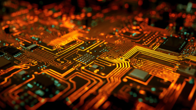
The rapid advancements in technology are fundamentally reshaping the landscape of electronics, with PCB printed circuit board innovation at the forefront of this evolution. According to a market research report by Fortune Business Insights, the global PCB market is projected to reach $86.04 billion by 2026, growing at a CAGR of 3.8% from 2019 to 2026. This growth underscores the critical role of PCBs in various applications, from consumer electronics to automotive systems, and highlights the importance of embracing innovative technologies to meet the rising demands for efficiency, miniaturization, and enhanced performance. As industries continue to integrate smart technologies and automation, the future of PCB printed circuit boards is not only promising but essential for enabling the next generation of electronic devices and systems.

The Evolution of PCB Technology: From Traditional to Advanced Methods
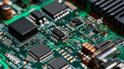
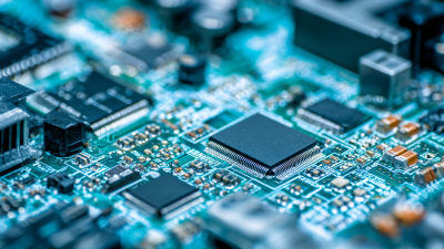
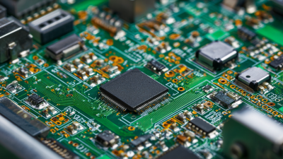
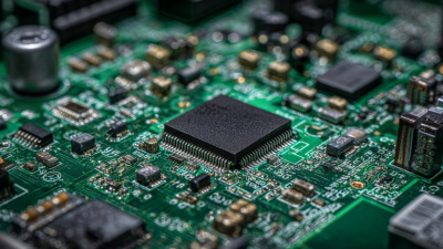
The evolution of PCB technology has witnessed remarkable transformations, moving from traditional manufacturing methods to sophisticated advanced techniques. Initially, printed circuit boards were predominantly produced using subtractive methods, where materials were removed to create the desired circuitry. This approach was labor-intensive and had limitations in terms of design complexity and durability. However, advancements in material science and fabrication techniques have ushered in an era where multi-layered boards and flexible designs are not only possible but commonplace.
Today, innovative methods such as additive manufacturing and embedded component integration are revolutionizing circuit board design. Additive manufacturing allows for the precise deposition of materials, enabling the creation of complex geometries that were previously unattainable. Furthermore, techniques like surface mount technology (SMT) have enhanced the efficiency of the assembly process, allowing for smaller, more reliable components that occupy less space—essential in our ever-more compact electronic devices.
As these advanced methods continue to evolve, they open new avenues for applications in industries ranging from consumer electronics to aerospace, driving the future of PCB technology to new heights.
Key Innovations Driving the Future of Printed Circuit Boards
The landscape of Printed Circuit Board (PCB) technology is rapidly evolving, driven by key innovations that optimize performance and enhance versatility across various applications. One significant trend is the integration of flexible and rigid-flex PCBs, which allows for high-density electronics in compact designs. These adaptable boards are ideal for consumer electronics and wearable devices, where space and weight are critical considerations. Their ability to bend without compromising functionality opens up new avenues for product design and applications in diverse industries.
Another groundbreaking advancement is the use of advanced materials in PCB manufacturing. High-frequency laminates and low-loss substrates enable better signal integrity and thermal management, crucial for high-speed data applications like 5G technology. Moreover, the introduction of eco-friendly materials aligns with the global push towards sustainability, making the manufacturing process not only efficient but also environmentally responsible. As these innovations continue to emerge, they pave the way for next-generation applications, from automotive systems to medical devices, reinforcing PCBs as a foundational element in modern electronics.
Exploring the Versatile Applications of PCBs in Modern Electronics
The ongoing trend of miniaturization in the electronics industry is transforming the landscape of printed circuit board (PCB) technology and applications. With the rising demand for smaller, more powerful, and feature-rich devices, PCB design is expected to accelerate into the era of intelligent computing. The PCB market is projected to grow significantly, with estimates indicating it will reach approximately $118.63 billion by 2031, up from $84.65 billion in 2024, reflecting a compound annual growth rate (CAGR) of 4.94%. This shift is vital as industries strive for efficiency and reliability in compact devices.
As devices shrink, the challenge of maintaining robust connectivity becomes imperative. Sensors, edge controllers, and mobile devices are continuously minimizing in size, necessitating innovative connectivity solutions. One effective approach is to integrate advanced design for test (DFT) techniques throughout the PCB manufacturing process, ensuring reliability without sacrificing space.
**Tip**: When designing PCBs for miniature applications, consider using high-density interconnection (HDI) technology, which allows for more components to fit into a smaller footprint, thus enhancing functionality and performance. Moreover, collaborating with reliable EDA and IP solution providers can significantly streamline the design process and mitigate potential issues related to space constraints.
Sustainability in PCB Manufacturing: Challenges and Solutions
The journey toward sustainability in PCB manufacturing is filled with challenges that manufacturers must navigate to align their processes with environmental goals. One significant issue is the reliance on hazardous materials in the production of printed circuit boards. Traditional PCBs often incorporate substances like lead and brominated flame retardants, which pose risks to both human health and the environment. As regulatory standards tighten globally, the industry is compelled to innovate and seek alternatives that reduce these impacts, prompting the development of eco-friendly materials and safer production techniques.
In response to these sustainability challenges, various solutions are emerging within the PCB industry. Manufacturers are increasingly adopting green practices, such as using biodegradable substrates, minimizing waste through lean manufacturing principles, and implementing recycling programs for defective boards. Additionally, advances in technology have paved the way for more energy-efficient production processes. By rethinking design and material choices, companies can not only comply with evolving regulations but also appeal to a consumer base that is progressively more environmentally conscious, ensuring a sustainable future for PCB technology.
Tips for Choosing the Right PCB Technology for Your Project
Choosing the right PCB technology for your project is critical to ensuring both performance and cost-efficiency. First, consider the specific requirements of your application, such as signal integrity, thermal management, and environmental conditions. For high-frequency applications, for example, materials with lower dielectric constants, like Teflon or Rogers, might be beneficial to minimize signal loss. Additionally, if your project demands high-density interconnections, opting for advanced techniques like microvias or blind/buried vias can greatly enhance your board's performance.
Budget is another crucial aspect when selecting PCB technology. Different manufacturing processes, such as traditional subtractive methods versus more modern additive techniques, can vary significantly in cost. Assess your project's scale and production volumes, as this will influence the choice of material and fabrication techniques. Moreover, prioritize working with a manufacturer that provides flexibility in technology options, allowing you to test prototypes and adjust designs as needed without incurring significant costs. Balancing technical requirements with budgetary constraints will pave the way for a successful PCB design tailored to your specific project needs.
Embracing Innovation: The Future of PCB Printed Circuit Board Technology and Applications
Dimension | Details |
---|---|
Material Types | FR-4, CEM-1, flexible substrates |
Layer Count | Single-sided, double-sided, multilayer |
Manufacturing Process | Etching, plating, solder masking |
Design Software | Altium Designer, Eagle, KiCAD |
Applications | Consumer electronics, automotive, medical devices |
Challenges | Complexity, cost, reliability |
Trends | Miniaturization, IoT integration, sustainable materials |
Related Posts
-
Solutions for Sourcing the Best PCB Circuit Boards Globally: Your Comprehensive Guide
-
7 Essential Tips for Sourcing the Best PCB Production Worldwide
-
Understanding the Industry Standards Challenges for Best PCB Circuit Production
-
How to Choose the Best PCB Board for Your Project Needs
-
Discover the Excellence of Best PCB Make from Top Quality Manufacturers in China
-
Mastering PCB Prototyping Techniques for Beginners in Electronics