
Blog
Top 10 Flex PCB Manufacturing Types How to Choose?
Choosing a flexible circuit begins with understanding the application, not the supplier’s catalog. A camera hinge, medical sensor, and automotive display need different mechanical and electrical solutions. This guide examines ten major flex PCB manufacturing types, including single-sided, double-sided, multilayer, rigid-flex, and high-density designs.
The market is expanding quickly. Grand View Research reports strong double-digit growth for flexible printed circuit boards through 2030, driven by smartphones, wearables, vehicles, and compact medical devices. Prismark’s semiconductor and PCB industry analyses also identify flexible and rigid-flex technologies as important growth areas in advanced electronics. These reports indicate opportunity, but they do not remove engineering risk.
IPC standards remain essential.
IPC-2223 provides design guidance for flexible and rigid-flex printed boards. IPC-6013 addresses qualification and performance requirements for flexible circuits. These references help buyers evaluate copper type, bend radius, coverlay, adhesive systems, impedance control, and reliability testing.
In practical sourcing, a thin board can look attractive until repeated bending exposes cracks near plated vias. A rigid-flex assembly may reduce connectors, yet its tooling and material costs can rise sharply. A simple single-sided circuit may outperform a complex multilayer design when space and signal demands are modest.
There is no universal best type.
The right choice depends on bend frequency, layer count, current capacity, temperature, assembly method, certification needs, and production volume. This overview compares each option through those criteria. It also highlights trade-offs that supplier brochures often simplify. Some recommendations may require adjustment after prototype testing, because laboratory assumptions rarely match every installation.
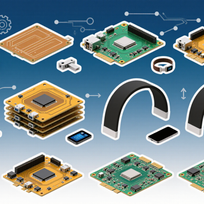
Flex PCB Types Explained: 10 Structures from Single-Sided to Rigid-Flex
Flex circuits solve problems that rigid boards cannot. They bend around hinges, cameras, and narrow battery compartments. The ten common structures include single-sided, double-sided, multilayer, sculptured, double-access, back-bared, shielded, adhesive-less, HDI flex, and rigid-flex. Each construction changes bend radius, thickness, impedance, yield, and repair difficulty. A single-sided circuit suits simple sensor wiring. A multilayer or HDI flex handles dense signals, but alignment becomes less forgiving. Rigid-flex combines stable component areas with flexible interconnects.
Industry data supports careful selection. The IPC North American PCB Statistical Program reported continued demand across high-reliability electronics, including aerospace, medical, and automotive applications. A 2024 market analysis by Grand View Research estimated the global flexible electronics market would expand strongly through 2030, driven by wearables and compact devices. These figures do not guarantee every flex project will succeed. Design details still decide outcomes.
In factory reviews, I check the bend zone first. A 0.2-millimeter coverlay edge can create stress concentration near a connector. Copper grain direction, neutral-axis placement, and dynamic-cycle testing matter more than a glossy prototype. Shielded flex reduces interference, while back-bared construction improves contact access. Adhesive-less layers can reduce thickness, but processing control becomes stricter. I once saw a rigid-flex design pass electrical testing yet fail after repeated folding. The missing test was mechanical cycling. A useful choice compares routing density, bend frequency, thermal exposure, assembly access, and expected service life—not only the initial quotation.
Top 10 Flex PCB Manufacturing Types: Copper-Layer Comparison
The chart compares representative copper-layer counts used in common flexible and rigid-flex PCB structures. Actual layer counts vary by circuit density, current capacity, impedance requirements, and mechanical design.
Single-sided structures generally provide the highest flexibility and lowest manufacturing complexity, while multilayer flex and rigid-flex structures support higher routing density but require more complex fabrication and material control.
Layer Count, Bend Radius, and Copper Thickness: Compare Key Specifications
Top 10 Flex PCB Manufacturing Types How to Choose?
Layer count, bend radius, and copper thickness should guide flex PCB selection. A single-sided flex circuit suits simple, low-cost routing. Double-sided designs support denser connections but bend less freely. Multilayer flex offers compact wiring, yet each added layer increases stiffness, registration risk, and fabrication cost. Rigid-flex combines stable component areas with flexible interconnects. It saves connectors, but poor transition geometry can cause cracking.
Bend radius needs physical testing, not guesswork. IPC-2223 guidance commonly starts static bends around six to ten times the finished thickness. Dynamic applications usually require a larger radius and controlled neutral-axis design. A 0.15 mm circuit may therefore need at least 0.9 mm static clearance. That is only a starting point. Real assemblies include coverlay, adhesive, stiffeners, and copper features. A 2024 flexible-electronics market analysis from Grand View Research estimated the sector at roughly US$35 billion in 2023, showing why specification discipline matters. Copper thickness also changes performance. One-ounce copper measures about 35 micrometres, while half-ounce copper measures about 17 micrometres. Thinner copper bends better but carries less current and dissipates heat less effectively. IPC-2223 and IPC-2152 calculations can support trace sizing, although laboratory validation remains necessary. Engineers sometimes overvalue minimum thickness. That choice can fail after repeated folding. A practical design may use thinner copper in the bend zone and thicker copper near connectors. Mistakes remain possible. Mechanical prototypes reveal them early.
Manufacturing Methods: Etching, Laser Drilling, and Sequential Build-Up
Etching remains a practical method for forming copper traces on flexible circuits. A resist pattern protects selected areas, while chemical solution removes exposed copper. It suits repeatable designs with moderate line widths and stable production volumes. However, narrow traces can lose accuracy when undercutting occurs. Engineers should check copper thickness, trace spacing, and bend zones before approving the artwork. A visual sample can expose problems that software misses.
Laser drilling creates small, controlled vias through polyimide and copper layers. It is useful when compact routing requires dense interconnections. Drill diameter, pulse energy, and surface treatment affect hole quality. Excessive heat may leave rough edges or damaged dielectric material. Operators should inspect hole walls and confirm reliable copper connection during process validation. Tiny holes look efficient, but they demand tighter controls.
Sequential build-up adds layers gradually instead of pressing every layer together at once. This approach supports high-density circuits and shorter connection paths. Each cycle requires accurate alignment, clean bonding, and careful registration checks. A slight shift can reduce annular rings and weaken later drilling results. Sequential build-up offers powerful design freedom, yet it increases process steps and inspection demands. Not always. The best choice depends on bend radius, layer count, current load, tolerance, and expected production volume. A design that works in a prototype may become expensive or unstable during repeated flexing. Engineers should compare yield data, cross-sections, and real bending tests before selecting the manufacturing route.
Manufacturing Methods: Etching, Laser Drilling, and Sequential Build-Up
| No. | Flex PCB Manufacturing Type | Typical Structure | Etching Method | Laser Drilling | Sequential Build-Up | Typical Layer Count | Typical Finished Thickness | Typical Minimum Trace / Space | Flexibility & Best-Fit Applications |
|---|---|---|---|---|---|---|---|---|---|
| 01 | Single-Sided Flex PCB | One copper layer on a polyimide or polyester dielectric with a coverlay. | Subtractive etching of rolled-annealed or electrodeposited copper; simplest process flow. | Usually not required for conductor formation; mechanical or laser cutting may be used for openings. | Not normally used | 1 copper layer | 0.10–0.25 mm | 0.10–0.15 mm | Excellent bending performance; suitable for displays, keyboards, sensors, and simple interconnects. |
| 02 | Double-Sided Flex PCB with PTH | Two copper layers separated by flexible dielectric and connected with plated through-holes. | Standard imaging and copper etching on both sides, followed by through-hole plating. | Laser drilling can create coverlay or micro-opening features; through-holes are commonly mechanically drilled. | Limited or none | 2 copper layers | 0.20–0.40 mm | 0.10–0.15 mm | Good flexibility and routing density; used in cameras, medical instruments, controls, and compact electronics. |
| 03 | Double-Sided Flex with Microvias | Two conductive layers using laser-formed microvias through a thin dielectric or coverlay. | Fine-line subtractive etching with controlled copper thickness and tighter registration. | UV laser drilling is used for small blind or coverlay openings, commonly about 50–100 µm in diameter. | Selective sequential processing | 2 copper layers | 0.18–0.35 mm | 0.075–0.125 mm | Higher routing density while retaining useful flex life; suitable for mobile, wearable, and optical modules. |
| 04 | Multilayer Flex PCB | Three or more copper layers laminated with flexible dielectric layers and coverlay. | Repeated imaging, lamination, registration, and etching steps; yield decreases as layer count rises. | Laser drilling is often used for coverlay openings and selected blind microvias. | Common for advanced routing | 3–6 copper layers | 0.30–0.80 mm | 0.075–0.125 mm | Balances routing density and flexibility; used for high-pin-count modules and space-constrained assemblies. |
| 05 | Rigid-Flex PCB | Rigid FR-4 or similar sections joined to one or more flexible polyimide sections in one board. | Etching is performed on rigid and flexible portions with different copper and dielectric constructions. | Mechanical drilling is common in rigid zones; laser drilling supports microvias and flexible-zone openings. | Frequently used | 2–16 total layers | 0.50–2.00 mm | 0.075–0.125 mm | High mechanical reliability and fewer connectors; used in aerospace, automotive, medical, and industrial electronics. |
| 06 | Dynamic-Flex PCB | Thin, highly bendable flex construction designed for repeated movement in a controlled bend zone. | Uses thin rolled-annealed copper and carefully controlled etching to reduce stress concentration. | Laser drilling is generally limited to openings and small interconnect features outside the active bend area. | Normally minimized | 1–2 copper layers | 0.10–0.30 mm | 0.10–0.15 mm | Best for repeated folding, sliding, or rotating applications such as hinges, print heads, and moving sensors. |
| 07 | High-Density Interconnect Flex | Fine-line flex or rigid-flex construction using small pads, blind microvias, and dense fan-out routing. | High-resolution imaging and controlled-depth etching are required to maintain narrow conductors. | UV laser drilling is central to microvia formation, with typical finished openings of about 50–100 µm. | Core manufacturing method | 2–8 copper layers | 0.25–0.80 mm | 0.050–0.100 mm | Very high interconnection density; suitable for compact computing, medical, camera, and wearable devices. |
| 08 | Chip-on-Flex (COF) Circuit | Thin flex substrate with bare semiconductor die attached directly by flip-chip or thermocompression methods. | Fine-line etching forms the die bonding fingers and signal routing on thin copper. | Laser drilling may form coverlay openings and fine-pitch access features. | Often used for fine-pitch fan-out | 1–3 copper layers | 0.05–0.20 mm | 0.040–0.075 mm | Extremely thin and compact; common in display drivers, imaging modules, and space-limited consumer electronics. |
| 09 | Metal-Core or Heat-Spreading Flex | Flexible circuit combined with a localized metal stiffener or thermal spreader rather than a fully flexible stack. | Etching forms the flex circuitry; metal stiffeners are separately patterned or mechanically processed. | Laser drilling can create precise openings through coverlay and thin stiffener interfaces. | Application-dependent | 1–4 copper layers | 0.30–1.20 mm | 0.10–0.15 mm | Provides localized heat dissipation and mechanical support; useful for power LEDs, sensors, and compact power modules. |
| 10 | Ultra-Thin Wearable Flex PCB | Thin single- or double-sided polyimide circuit with low-profile coverlay and compact components. | Thin-copper etching minimizes overall thickness while maintaining adequate signal and power paths. | Laser drilling is preferred for small openings, fine-pitch pads, and miniature via structures. | Used selectively | 1–2 copper layers | 0.08–0.25 mm | 0.075–0.125 mm | Lightweight and conformable; suitable for health monitors, smart accessories, compact sensors, and connected devices. |
Reliability Benchmarks: IPC-2223 Bend Rules and 10,000-Cycle Testing
Flex PCB reliability depends less on appearance than on how the circuit bends in real use. IPC-2223 provides construction guidance, but it does not offer one universal bend radius. The correct radius depends on layer count, finished thickness, copper geometry, and whether the bend is static or dynamic. A thicker stack-up usually needs more space. Sharp corners need attention.
In production reviews, I check the neutral axis, stiffener transition, and exposed copper near the bend zone. I also inspect whether adhesive squeeze-out creates a hard edge. That small edge can become a crack starter. For dynamic designs, the bend radius should be validated through controlled testing, not selected from a drawing alone. I record fixture radius, travel speed, bend angle, temperature, and electrical resistance during each cycle.
A 10,000-cycle test can reveal failures that visual inspection misses. The sample should flex repeatedly under its intended load, with continuity monitored throughout testing. Afterward, technicians should examine copper traces and plated vias under magnification. Ten thousand cycles is useful evidence, not a guarantee. My earlier reviews sometimes treated the cycle count as the final answer. That was too simple. Production variation, assembly pressure, and field contamination can change results. A reliable supplier should provide test records, sample identification, and clear pass-fail limits before selecting a flex PCB manufacturing type.
How to Choose: Match Flex Type, Cost, Density, and Application Requirements
Choosing a flex PCB starts with the application, not the lowest quotation. Single-sided boards suit simple sensor links and short dynamic paths. Double-sided designs support denser routing, but they need tighter bend control. Multilayer flex circuits save space when signals, power, and grounding must share a narrow profile. Rigid-flex combines stable component areas with flexible connections. It often reduces assembly joints, though its tooling cost can rise quickly.
Match the flex type to movement, density, and electrical demand. A wearable device may need thin polyimide, small bend radii, and repeated flexing. A camera module may prioritize precise folding and controlled impedance. High-density routing requires smaller vias and careful stackup planning. Those features increase fabrication difficulty. Keep the bend zone free of components and abrupt copper transitions. Copper should not be unnecessarily wide near a hinge.
Cost comparisons can mislead. A cheaper single-sided board may require extra connectors, cables, and assembly labor. A multilayer design may cost more per panel but reduce total system space. I once underestimated the impact of stiffener placement, and the prototype bent unevenly. That mistake exposed a useful lesson: mechanical review must happen before final routing. Ask the manufacturer about bend-cycle testing, material tolerance, adhesive behavior, and inspection limits. Do not approve a design from electrical files alone. A practical prototype should reflect production tooling, actual folding conditions, and the intended service temperature.
Related Posts
-
Top 10 Flex Circuit Board Manufacturers for Global Buyers
-

Top PCB Suppliers for Quality Circuit Boards in 2026?
-
Future Trends of Flex Circuit Board at 2025 China Import and Export Fair Insights and Data
-
How to Master Circuit Board Design: Essential Tips for Beginners
-
Unlocking Innovation: A Beginner's Guide to Circuit Board Design Techniques for Modern Electronics
-

Why PCB Make is Essential for Your Electronics Projects: Unlocking Innovation